Presentation
KiCad is a powerful open-source electronics design automation (EDA) suite that offers a range of tools for schematic capture, integrated circuit simulation, printed circuit board (PCB) layout, and 3D rendering. One of the key advantages of KiCad is its support for action plugins and an extensive Python scripting API, which provide users with a high degree of customization and flexibility.
This article showcases and discusses the technical implementation of two plugins I developed to improve the workflow with this tool:
- KiCad Auto Silkscreen Placer: a tool to automatically move all the silkscreen part designators to a place where they are readable. Jump to section...
- KiCad Pinout Generator: a tool to export the pinout of components from the PCB to various formats such as C/C++ code, FPGA constraints files, CSV, etc. Jump to section...
Additionally, we'll highlight other plugins that I have contributed to or recommend for KiCad users.
Whether you're an experienced PCB designer or just starting out, these plugins are sure to improve your workflow and help you create more efficient designs.
KiCad Auto Silkscreen Placer plugin
![]()
Plugin description
This KiCad plugin automatically computes a position for all silkscreen reference designators that is free of overlap with other PCB elements (footprints including their reference designators, solder mask, vias, PTH/NPTH holes, etc.). It saves a lot of time over doing it entirely manually.
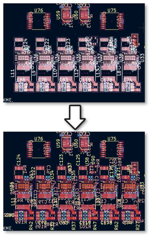 Example before/after result of this plugin.
It is intended to be used after laying out and routing a board to place most of the designators in an adequate position. Some manual work might still be required to improve the look of the silkscreen but the heavy lifting should be done!
It also positions the value field when it is placed on a silkscreen layer.
Download and usage instructions
This plugin is not yet released on the plugin and content manager. It will be submitted when it reaches the "V1.0" milestone.
This is the link to the GitHub repository for the project: https://github.com/CGrassin/kicad-auto-silkscreen
It includes usage instruction. Please report any issue you encounter while using this plugin on GitHub.
Clip of Auto Silkscreen Placer moving reference designators on a board
Technical implementation details
This plugin determines a position map with priorities for each footprint whose reference is to be moved, and then picks the best valid position.
Position map
The placement algorithm sweeps all possible positions for the silkscreen item, starting from the closest position to the courtyard's bounding box of a component. This figure shows a typical priority map generated by the plugin:
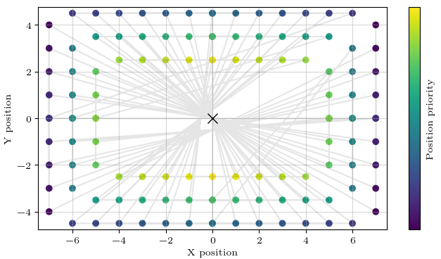 Position map; the component is at the center, each point is a possible position to be evaluated.
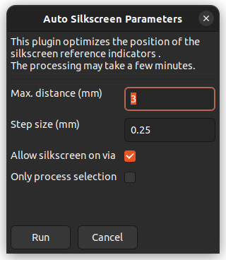
The parameters to generate this priority map are the maximum allowed distance and the step size. They have a direct impact on the performance of the plugin as detailed below.
Collision detection
Each position of the map is evaluated for validity. To achieve this, the plugin checks:
- If the item is contained within the board edges,
- If the item is colliding with any other item:
- Courtyard of parts,
- Other items on the same silkscreen layer, including user drawings and the reference designator of other parts,
- Solder mask,
- Through holes (e.g. mounting holes),
- Vias - this check is optional because depending on the manufacturing parameters, it may be perfectly valid to have silkscreen over the vias (with tented vias for instance).
To check for collision, the algorithm uses both simple rectangular bounding boxes and the effective shape. Bounding box can be used for straightforward shapes (e.g. overlap with a via) and is very fast. Using the effective shape is required for more complex shapes such as drawings, and is mandatory for ones that might be concave or contain holes such as courtyards.
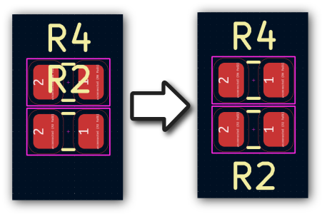 Example of a collision: the reference is overlapping with the courtyard before running the plugin.
Note: at this stage, the plugin tests for each position independently. It is planned for a future V2.0 of the plugin to try to nudge other reference designators around to find an optimum placement that minimizes the distance between each footprint and its reference.
Performance and optimization
The algorithm has a time complexity of O(n²), where n represents the number of items on the board. Without any optimizations, evaluating every item for every position would take a long time, especially for complex boards.
In my code, I've implemented a basic optimization strategy that involves filtering the PCB items within the maximum displacement area of the item that the plugin wants to move. Only the elements within this area are checked for collision, which saves time and enables the plugin to be used on designs with a large number of objects.
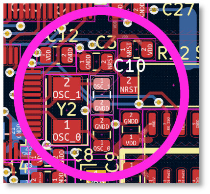 Optimization: only the items in the purple circle should be processed for collision for C10.
To determine the radius of this area, the algorithm takes into account the size of the part, the size of the reference indicator (and value field if it is on the silkscreen layer), and the maximum allowed displacement. Any item whose bounding box center is closer than this radius is considered for collision. The image above shows an example of this optimization, where only the items in the purple circle should be processed for collision when trying to find a position for C10.
User interface
The user interface is a simple WX dialog built with wxFormBuilder that enables users to change the settings and launch the computation.
 The plugin's settings user interface.
Additionally, the user interface offers a command-line interface (CLI) for more advanced users.
KiCad Pinout Generator plugin
![]()
Plugin description
The KiCad Pinout Generator plugin generates pinouts of components from a PCB file in various formats. These include:
- Text formats for documentation:
- Markdown table
- HTML table
- CSV
- Tab-separated list
- WireViz
- Code format for software development:
- C/C++ enums
- C/C++ #define
- Python/MicroPython dict.
- Xilinx XDC constraint (FPGA)
- Microsemi PDC constraint (FPGA)
Example applications include automatically creating the pin assignment from a microcontroller to C code and generating interface documents for connectors.
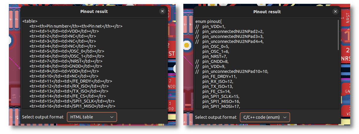 Example of a export as HTML (left) and C/C++ enum (right)
It is very convenient to use this plugin instead of manually extracting information. This effectively eliminates the risk of errors, saves time, and helps keep information up to date.
This plugins only gives useful output if the pins have net names. Use labels in the schematic editor to give the nets a human-readable name.
Download and usage instructions
This plugin is available on the Plugin and Content Manager.
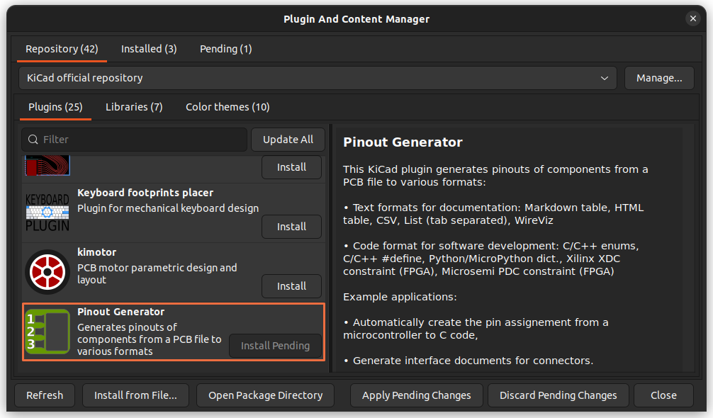 The plugin in KiCad's Plugin and Content Manager.
For the latest development versions or to raise issues/request features, this is the plugin's GitHub repository: https://github.com/CGrassin/kicad-pinout-generator
Note: the codebase is considered in a stable state, but feature requests such as new output formats are very welcomed.
Technical implementation details
The KiCad Pinout Generator plugin uses the Python scripting API to read the selected footprint and access the properties of all its pads.
The output processing depends on the selected format. For example, when generating C/C++ code, the plugin ensures that the code is valid and will compile without errors. In code formats, power pads and unconnected pins, which are usually not relevant, are excluded.
Here is an example of a microcontroller as input in the schematic tool, and the output in C/C++ define format:
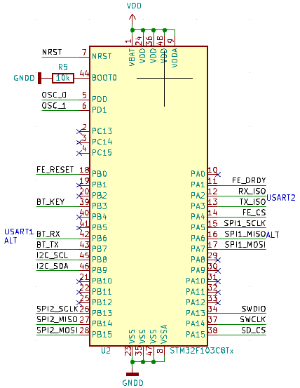 A microcontroller with pin assignments in Eeschema.
This is the output of the C/C++ define format:
// Pinout for U2 (STM32F103C8Tx)
#define I2C_SDA PB9
#define I2C_SCL PB8
#define BT_TX PB7
#define BT_RX PB6
// #define UNCONNECTEDNU2NPAD41 PB5
// #define UNCONNECTEDNU2NPAD40 PB4
#define BT_KEY PB3
// ...
And here is the output in Markdown table format (directly copied to this article and rendered by Parsedown):
| Pin number | Pin name | Pin net |
|---|---|---|
| 46 | PB9 | /I2C_SDA |
| 45 | PB8 | /I2C_SCL |
| 43 | PB7 | /BT_TX |
| 42 | PB6 | /BT_RX |
| 41 | PB5 | NC |
| 40 | PB4 | NC |
| 39 | PB3 | /BT_KEY |
| ... | ... | ... |
The Pinout Generator plugin is versatile and can be used on connectors for generating interface control documents (ICDs). In addition to creating simple tables of pins, it offers a "WireViz" export format that enables quick generation of wiring diagrams and harness specifications, as shown in the example below.
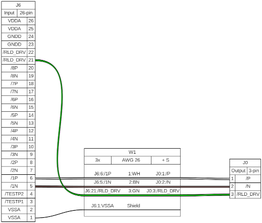 Example WireViz render using the output of this plugin.
In the example above, the plugin generates the pinout for the connector on the left, which is part of the PCB. The other connectors and wires are simulated data used for demonstration purposes.
Other recommended plugins
I have contributed to the code of other plugins that I also recommend:
- Actions scripts: Generates via stitching and circular zones. I contributed several bugfix pull requests (including the KiCad 7 port) and a new feature.
- RF tools: A collection of tools for RF PCB design, such as via fencing generator. I contributed several bugfix pull requests (including the KiCad 7 port).
Additionally, these are other plugins I use:
- Interactive BOM: Generates a convenient BOM listing with the ability to visually correlate and easily search for components and their placements on the PCB.
- Replicate layout: Replicates the PCB layout of one hierarchical sheet to other hierarchical sheets.
- Eagle Dark Theme: A dark theme for the schematic capturing tool inspired by Eagle CAD.
Auteur : Charles Grassin
What is on your mind?
Sorry, comments are temporarily disabled.
No comment yet!