Introduction
Homemade PCB manufacturing is a great way to get inexpensive board prototypes with no delay. Starting with raw boards, the challenge is to precisely remove the copper layer where it shouldn't be. Mechanical etching is one solution but it tends to be tricky and uses a CNC mill. Chemical etching is usually more consistent but it can be messy and requires a way to mask the board with an etch resistant material.
In this article, I show the method I came up with to get reliable, fast and precise PCBs with no headaches using a 3D printer, a permanent marker and any etchant. This process is in two parts:
- Masking the board
- Etching the board
Part 1: masking the board
Masking the board is the trickiest part of DIY PCB etching. There are several ways, most of which I have used with questionable results and/or reliability: hot toner transfer, heatless toner transfer, laser masking removal, etc.
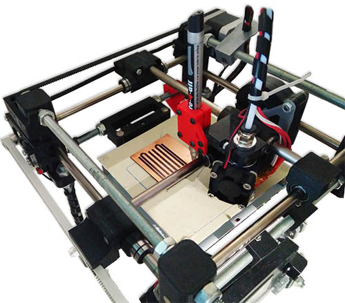
My method uses a permanent marker attached to a 3D printer to directly plot the mask onto the PCB. Although it does not achieve the same kind of resolutions as you get with some of the other method, it is really easy to set up.
Step 1: designing your PCB
The first obvious step is to design your PCB in an EDA : I use KiCad (Open-Source, cross-platform). The most important thing to do here is to set the design rules prior to the PCB routing :
- Minimum track width: the width of the tip of your marker (or a little more to be on the safe side). This can be as low as 0.2mm/8mil.
- Minimum track spacing: depends on the XY resolution of your printer. 8mil is a reasonable assumption to get repeatable results.
Step 2: converting the file
To be able to send the board design to a CAM package, we need to convert it to an SVG file. In most EDAs (including KiCad), this is easy to do with a "Export as SVG" button. If you have multiple layers, generate a file for each layer.
Next, we need to process the complex SVG with multiples path, objects, layers, group, etc. to convert it into a single path simple SVG. You need to open your SVG into Inkscape (Open-Source, cross-platform), and perform the following series of commands: CTRL+A (Select all), CTRL+U (Ungroup), CTRL+MAJ+C (Convert object to path), CTRL+D (Duplicate), CTRL+ALT+C (Convert stroke to path), CTRL+A (Select all), CTRL+U (Union) and CTRL+MAJ+R (Fit page to content). You can then save this file in simple SVG format.
Step 3: generate the Gcode
The Gcode gives the instructions to the 3D printer. Usually, a slicer generates it (Cura, Slic3r,...). In this case, we will be using a CAM software to achieve this. Jscut (Open-Source, cross-platform, web-based) is a simple CAM package that does just that: jscut.org.
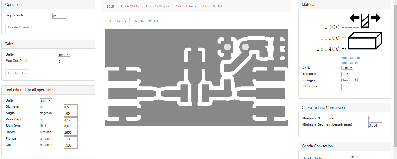
On the first use, you will need to set its configuration, here is mine: download it. This is what you must set:
- Diameter: the diameter of the tip of the marker,
- Step Over: 0.8
- Rapid (the movement speed when moving over the board): about 2500 mm/min
- Cut (the movement speed when drawing on the board): 1000 to 1500 mmm/min
- Clearance (the clearance when moving over the board): 1 mm
When you're done configuring:
- Open the SVG in jscut,
- Select the SVG,
- Create an operation: pocket, 0.001mm deep,
- Click on "Generate",
- Save the GCODE.
Step 4: plotting the mask
Now that we have the toolpath ready, we can do the masking;
- Stick the PCB on the 3D printer bed,
- Home your printer and disable the steppers,
- Place the pen on the 3D printer head and manually move it so that it barely touches the top right side of your PCB. Make sure the 3D nozzle clears the board. Enable the steppers,
- Run the Gcode on your printer (either move the Gcode file on a SD card or directly send it to your machine using printrun)!
 This whole process may seem lengthy but it actually only takes about 5 min; definitely worth a try!
Part 2 : etching process
There are various ways to etch copper of PCB. I personally use a ferric chloride bath. It is very reliable and easy but it does have one drawback: it is nasty for the environment and must be disposed of accordingly (refer to local laws).
This is how I proceed:
- Because I order ferric chloride as a powder, I first need to prepare the solution. I dissolve 3g per 10ml of warm water (about 45°C), in a glass container.
- Put the masked PCB in the solution. It needs to be fully dipped in the liquid.
- Move the board while it is etching.
- As soon as the copper fully disappears from the board, take it out of the bath and give it a good wash with water.
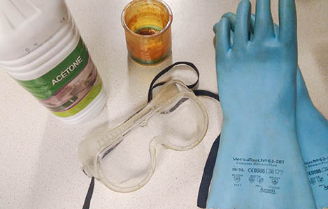
- To get rid of the permanent marker, wash the board with acetone or alcohol.
Your board is done!
Results gallery
These boards are done using this method. I will add more as I get better at this process.
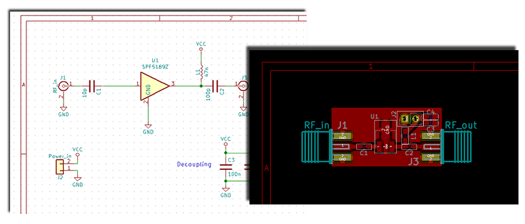
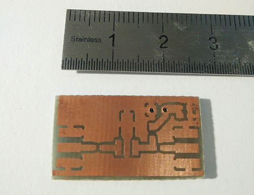 A LNA circuit
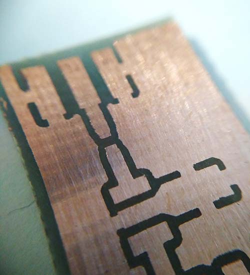 Details of the board
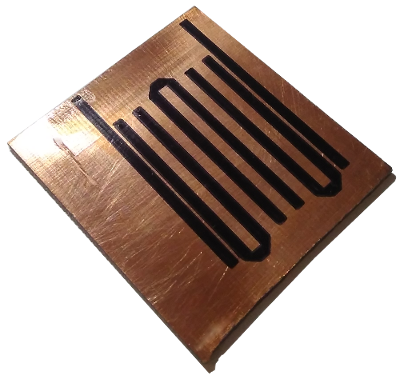 A masked hairpin filter board, before the etching process.
Author: Charles Grassin
What is on your mind?
Sorry, comments are temporarily disabled.
#1 Spifthespa
on April 6 2020, 14:33
#2 Author Charles
on April 7 2020, 10:15
#3 sagan
on August 6 2020, 9:34
#4 Gregoire Mazarakis
on August 27 2020, 16:59
#5 ss5r
on November 9 2020, 18:45
#6 Author Charles
on November 10 2020, 7:31
#7 PquOeR
on November 5 2023, 6:56
#8 Veishen
on August 28 2024, 3:40