Overview
These passive RF differential probes offer a cost-effective way to perform in-circuit measurements on RF systems, in situations where a dedicated test port is unavailable, with minimal impact on the device under test.
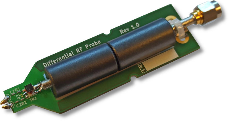
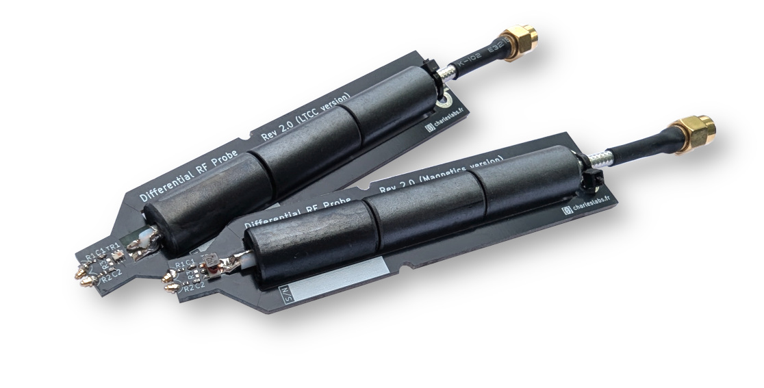 Figure 1: PCBs of the rev 2.0 of the RF probe (two variants).
The probe's spring-loaded pins can be positioned at any angle to fit the ground-signal track spacing, with a practical lower bound of 1 mm, equivalent to the length of an 0402 component.
Compared to commercial active probes, this probe is significantly more affordable and has a different input power range, making it suitable for use on high-power RF circuits for instance. A typical application for this probe is for tuning multiple-stage RF power amplifiers.
Rev 2.0 is available in two variants:
- Magnetics variant, using the TCM1-63AX+ transformer, targeting a wide bandwidth with high flatness.
- LTCC variant (experimental), using the NCS1-332+ transformer for higher input power and slightly improved performance on a narrower bandwidth.
The total bill of materials (BOM) cost is under $15 per unit in single quantity.
I am grateful to my former employer PTS GmbH for their support and resources during the development of this project, as well as for allowing me the freedom to continue working on it independently.
Performance
This table lists the key characteristics of the two rev 2.0 variants, measured with R = 100 Ω, with DC block capacitors:
| Parameter | Magnetics variant | LTCC variant |
|---|---|---|
| Usable frequency range | 400 MHz to 2.5 GHz | 400 MHz to 2.5 GHz |
| Transfer coefficient at 1 GHz * | -19.5 dB | -20.9 dB |
| Flatness over 100 MHz | < 0.9 dB | < 1 dB |
| Loss for the DUT at 1 GHz * | < 0.4 dB | < 0.4 dB |
| Maximum input power * | > 1 W to 8 W | > 15 W to 50 W+ |
| DC protection | 50 Vdc | 50 Vdc |
(*) Note: these values depend on the value of series resistors R1 and R2. The values given in this table are for R = 100 Ω. See the sections Principle of operation and Simulation below for an analysis of the effect of this parameter on performance. The maximum input power is for the full resistance range.
The upper bandwidth of the probe is limited to about 2.5 GHz due to the geometry.
Rev 2.0 introduces the following improvements over rev 1.0:
- Added 1 extra ferrite bead for improved handling (longer probe body) and more common noise rejection.
- Shortened the path from the pogo pins to the resistors (improved RF performance).
- Introduced an experimental second variant based on an LTCC transformer (Mini-Circuits NCS1-332+), in addition to the existing core-and-wire version.
Usage
This probe is designed to be used with a Vector Network Analyzer (VNA), Spectrum Analyzer, or Oscilloscope. To use it effectively, it is important to obtain the correction curve for the specific probe in order to take quantitative power measurements.
For instance, the typical recommended usage with a VNA is to first perform a through calibration with a reference terminated test track, and then probe RF lines as needed.
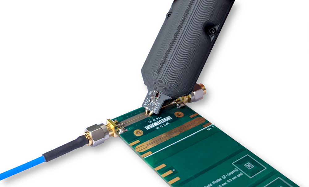 Figure 2: Example usage of the probe on a PCB microstrip transmission line.
All the files are in the GitHub repository: https://github.com/CGrassin/rf_differential_probe.
Note: when using with an oscilloscope, a 50 Ω termination is required (either internal for devices that support this feature, or externally as close to the input as possible).
Technical details
Principle of operation
This probe has a simple construction, as shown in the diagram below:
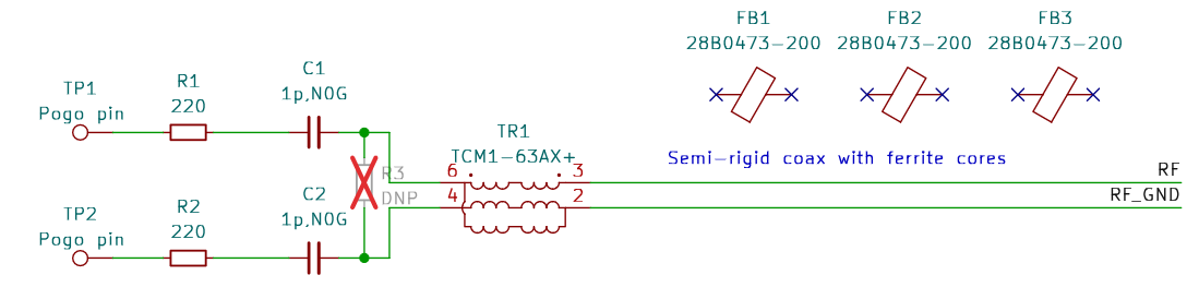 Figure 3: Circuit diagram of the RF probe in KiCad (magnetics version).
This is the principle of operation:
- TP1 and TP2 are spring-loaded probing pins that should be as short as possible.
- R1 and R2 limit the power going through the probe, setting its attenuation and load on the Device Under Test (DUT). They should have the same value, R1 = R2 = R.
- C1 and C2 block DC to protect the balun. They limit the lower bandwidth of the probe; 0 Ω resistors can be used instead if the probed RF track has no DC component. I measured the probe performance with and without these capacitors.
- TR1 is a balun to convert the input differential RF signal into a balanced output. It can be either a coil and wire balun, or LTCC.
- FB1 to FB3 are ferrite beads over a piece of coaxial cable acting as a common-mode choke to suppress low-frequency common-mode current from flowing on the outside of the coax shield.
The theoretical attenuation of R1 and R2 follows this equation (ignoring losses in the transformer and transmission line):

The two variants differ only in their transformer. This affects the usable frequency range and the transfer flatness, as detailed in the Performance and Measurements sections.
Simulation model
The simulation model was created using QucsStudio and uses the S-parameter file provided by the transformer manufacturer, with lumped component models for passives. Transmission line losses are not taken into account.
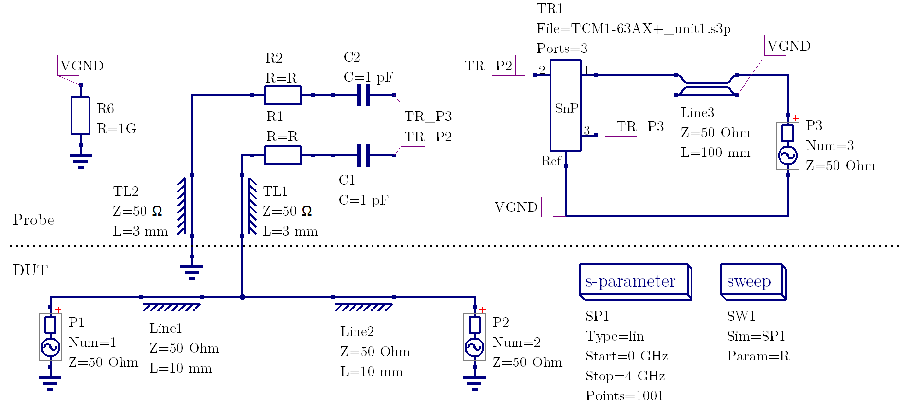 Figure 4: Simulation diagram for the probe in QucsStudio/uSimmucs.
The DUT has two ports, P1 and P2, while the output port of the probe is P3.
This simulation model can be used to modify various parameters, especially the values of the two resistors. For instance, the graph below shows a sweep of resistor values for all E6-series values between 100 Ω and 1 kΩ.
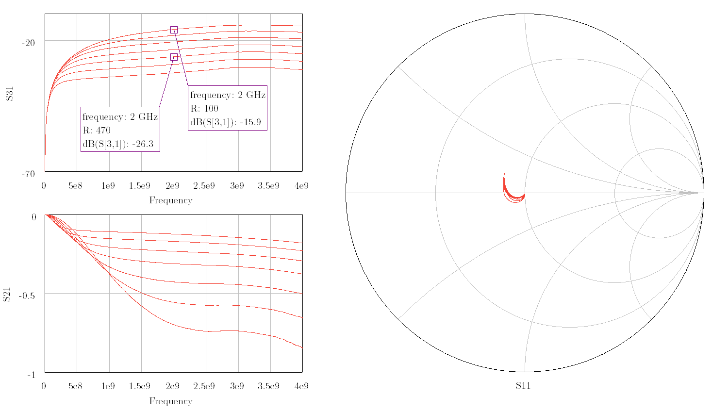 Figure 5: Simulation results of the probe in QucsStudio/uSimmucs.
The table below summarises the simulated key values for a sweep of E6-series resistor values between 100 Ω and 1 kΩ (with the TCM1-63AX+ balun):
| R value | Probe attenuation (S31) at 2 GHz | Effect on DUT (S21) at 2 GHz |
|---|---|---|
| 100 Ω | -16.1 dB | -0.6 dB |
| 150 Ω | -18.3 dB | -0.5 dB |
| 220 Ω | -20.8 dB | -0.4 dB |
| 330 Ω | -23.7 dB | -0.3 dB |
| 470 Ω | -26.4 dB | -0.2 dB |
| 680 Ω | -29.3 dB | -0.1 dB |
| 1000 Ω | -32.5 dB | -0.1 dB |
Design
The probes were designed in KiCad 10.
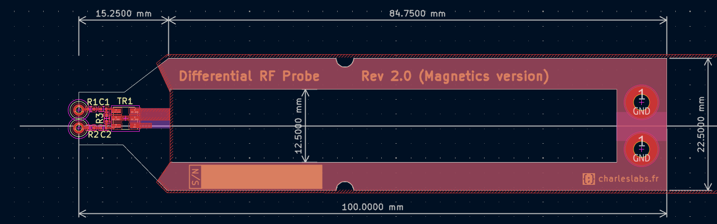 Figure 6: PCB of the probe in KiCad 10.
The pogo pin mounts are plated through hole (PTH) pads bisected by the board edge cut, which allows the pin angle to be freely adjusted to match the spacing of the target RF track. Two mounting holes at the rear of the board allow the SMA cable shield to be soldered directly and a zip tie to be added for strain relief.
The PCBs were manufactured by JLCPCB on standard 2-layer 1.6 mm FR4 with black solder mask.
A 3D-printed enclosure was designed to improve handling and prevent accidental contact with the RF components.
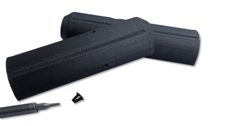 Figure 7: 3D-printed enclosure for the probe.
It is printed in PLA and assembled with 2 M2×6 mm screws.
Measurements
The measurements were performed using a LiteVNA 64 vector network analyzer and an example test track (50 Ω microstrip transmission line). The VNA is calibrated with short, open, load and through (SOLT) with the test track connected to port 1. R = 100 Ω for both variants.
Measurement principle
Three metrics were used to evaluate the performance of the probe:
- Probe transfer function — the attenuation from the line to the probe output (S31 in the simulation).
- Effect on the DUT — insertion loss — attenuation of the line due to the probe (S21 in the simulation).
- Effect on the DUT — return loss — reflection introduced at the line input by the probe (S11 in the simulation).
Transfer function of the probe
To measure the transfer function, the test track is terminated with 50 Ω and the power going through the probe is measured on port 2.
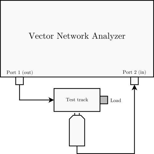 Figure 8: Setup #1 to measure the transfer function of the probe.
The measurements for both variants, with and without the DC block capacitors, are shown in the figure hereunder.
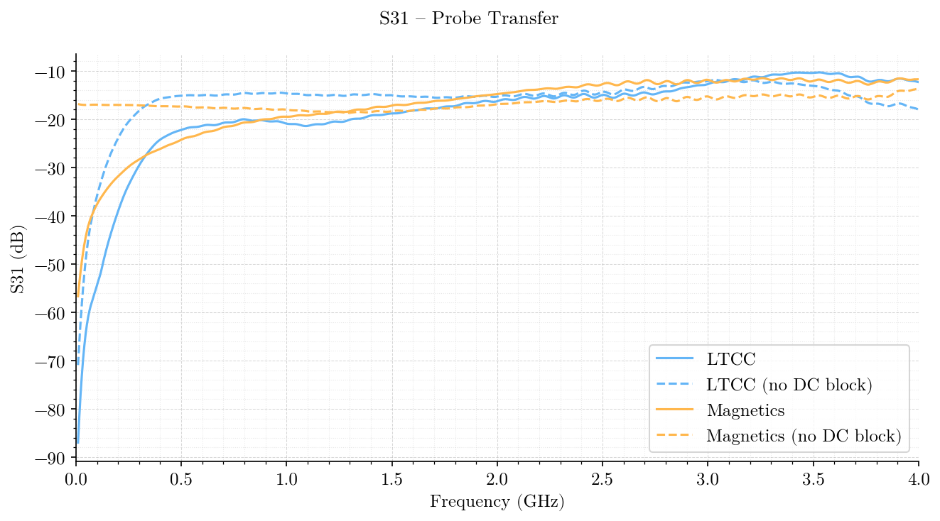 Figure 9: Transfer function (S31) of the two rev 2.0 variants.
This metric characterizes the sensitivity of the probe. The flatness indicates consistent sensitivity across frequency. The absolute value sets the calibration offset when taking power measurements.
Effect on the DUT — insertion loss
To measure the insertion loss caused by the probe, the probe is terminated with 50 Ω and placed on the test track while power transmission through the track is measured on port 2.
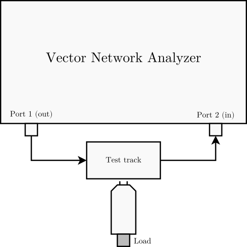 Figure 10: Setup #2 to measure the effect of the probe on the circuit.
The measurements for both variants, with and without the DC block capacitors, are shown in the figure hereunder.
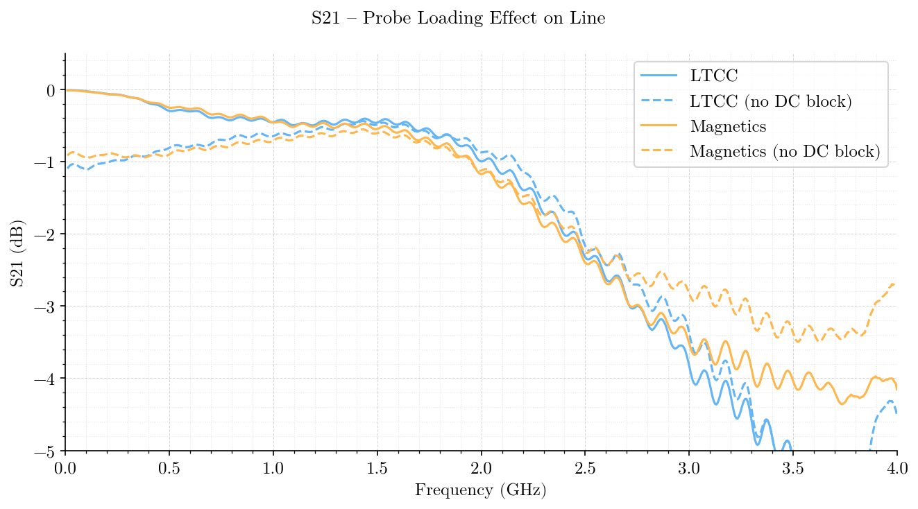 Figure 11: Insertion loss on the test track (S21) for the two rev 2.0 variants.
For this metric, a value closer to 0 dB indicates better performance (less effect on the DUT).
Effect on the DUT — return loss
S11 is measured using setup #2 to evaluate the return loss caused by the presence of the probe.
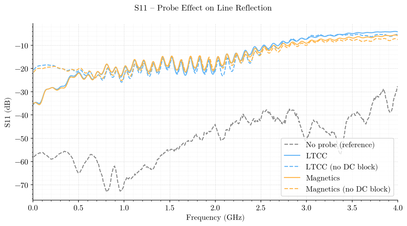 Figure 12: Return loss on the test track (S11) for the two rev 2.0 variants, compared to the baseline without probe.
For this metric, lower values indicate better performance (less return loss introduced by the probe).
Conclusion
This RF differential probe offers a practical and affordable solution for in-circuit RF measurements, particularly in situations where a dedicated test port is not available. It represents a compelling alternative to commercial probes, especially for high-power applications such as tuning multi-stage RF power amplifiers.
The magnetics variant covers a broad 400 MHz to 2.5 GHz range with good flatness, making it the more versatile of the two. The LTCC variant performs significantly better without the DC block capacitors than with them, making it the preferred choice for AC-only applications. It also offers higher maximum input power, which may be advantageous in power amplifier applications.
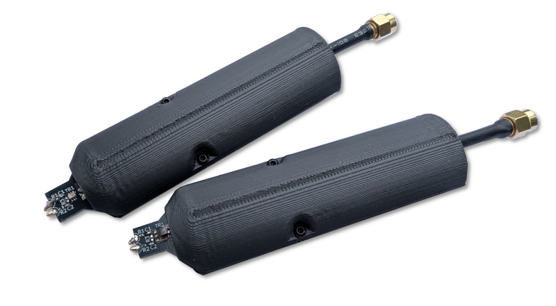 Figure 13: Two variants of the RF probes rev. 2.
The choice of series resistors R1 and R2 gives the user a straightforward way to trade off probe attenuation against loading effect on the DUT, allowing the probe to be adapted to a wide range of measurement scenarios. Combined with a proper VNA calibration using a reference test track, this probe is capable of accurate, quantitative power measurements across its usable frequency range.
All design files, including schematics, PCB layouts, simulation models, and the 3D-printable enclosure, are available in the GitHub repository for anyone wishing to build or further develop this probe.
Previous Revision (rev. 1)
This section describes the previous version of this project (rev. 1 of the electronics).
 Rev 1.0 of the RF probe.
Performance
This table lists the key characteristics of the probe:
| Parameter | Typical value |
|---|---|
| Usable frequency range | 500 MHz to 6 GHz |
| Attenuation at 2 GHz * | -22.5 dB |
| Maximum input power | > 44 dBm |
| Flatness over 100 MHz | < 1.5 dB |
| Loss for the DUT * | < 0.5 dB |
| DC protection | 50 Vdc |
Note: (*) These values depend on the value of series resistors. The values given in this table are for the baseline value of 240 Ω.
Measurements
Measurements were performed on a test track with two values for the resistors: R=100 Ω (ERJ-PA2F1000X) and R=240 Ω (ERJ-2RKF2400X).
Attenuation of the probe
To measure the attenuation of the probe (its transfer function), the test track is terminated with 50 Ω and the power going through the probe is measured on port 2.
The following figure illustrates this setup:
Setup #1: measuring the attenuation (transfer function) of the probe.
The following plot shows the probe attenuation measured using setup #1.
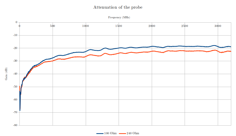 Plot of S31 for two values for the resistors.
For this metric, flatter is better. The absolute value characterizes the probe.
Loss on the test track due to the probe
To measure the loss on the test track due to the probe, the probe is terminated with 50 Ω and contacting the test track while the power going through the test track is measured on port 2.
The following figure illustrates this setup:
Setup #2: measuring the effect of the probe on the circuit.
The following plot shows the test track loss due to the probe (S21) measured using setup #2.
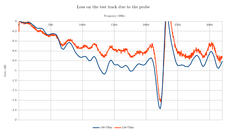 Plot of S21 for two values for the resistors.
For this metric, a value closer to 0 dB indicates better performance (less effect on the DUT).
Note: the large oscillation around 2.4 GHz is due to the measurement setup picking up external noise.
Return loss on the test track due to the probe
With either setup, S11 can be measured to evaluate the return loss caused by the presence of the probe.
The following plot shows the test track return loss due to the probe (S11) measured using setup #2.
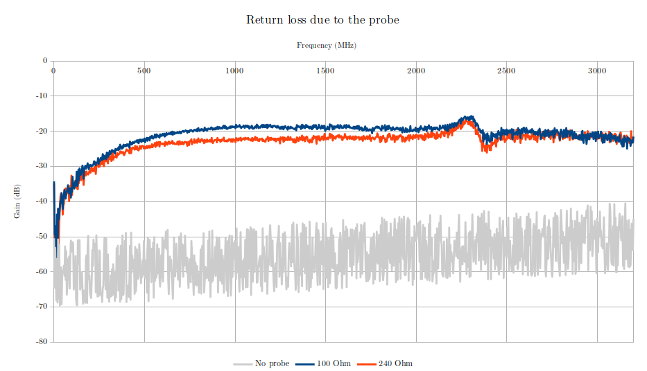 Plot of S11 for two values for the resistors.
For this metric, lower values indicate better performance (less return loss).
Limitations and future improvements
The rev 1.0 of this probe has a limitation in the maximum attenuation it can achieve due to sensitivity to radiated emissions. For the setup used in the measurements detailed above, the noise floor is about -30 dB, meaning that the maximum usable value of the resistors is R=1000 Ω.
Autor: Charles Grassin
What is on your mind?
Sorry, comments are temporarily disabled.
No comment yet!