Introduction
Microfluidics is an area of research based on the manipulation of small fluid volumes on the order of microliters, nanoliters or even picoliters. The main practical application is to create a lab-on-a-chip, a platform to perform medical diagnostics, environmental monitoring, and scientific research in a rapid, inexpensive, portable, and reliable environment [1][2].
The electrowetting-on-dielectric (EWOD) effect is the basis for this: droplets under an applied voltage tend to reduce their contact angle with a surface [3].
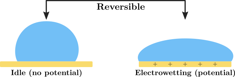 Demonstration of the electrowetting effect (blue = droplet, yellow = electrode with hydrophobic coating)
Using this effect, we can actuate the droplets with movement, mixing and splitting with clever electrode design. This allows us to create complex arrangements such as reservoirs, tracks, or even three-dimensional structures [4]. For instance, research as been carried out to develop DNA sequencing chemistry on an electrowetting‐based digital microfluidic platform [5].
I designed µDropplet, an inexpensive Arduino-based platform with an 8×8 array of electrodes driven by a high voltage to experiment with various microfluidics techniques and materials in the micro-liters range.
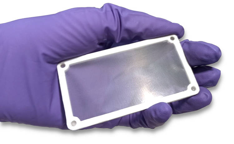
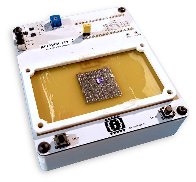 The µDroplet platform with a drop of blue dyed water on top of the hydrophobic film
This article describes the design, usage and some tests results obtained with this system.
Video
This video shows the project:
Design
My design is strongly inspired by GaudiLabs' OpenDrop platform.
This is a top level block diagram of the circuit:
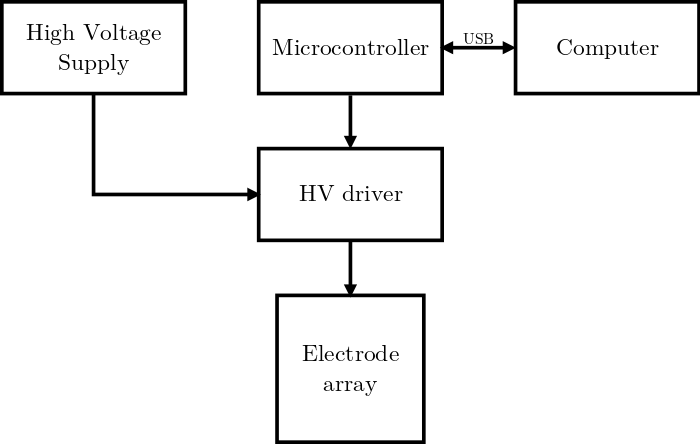 Block diagram of the circuitry of µDroplet
Electronic circuit
For the microcontroller, I chose to use an Arduino Nano development board with an ATMega328P.
The array driver chip is a HV507. It is a 64-channel serial-to-parallel converter with high-voltage push-pull outputs (up to 300 V). It is intended as a printer driver. This is by far the most expensive chip of the BOM.
The high-voltage supply is based on the "Nixie HV Switching PSU" by Nick de Smith, designed to power nixie tubes. It is able to output DC 80-275 V from a 5-16 V input. The potentiometer on my device sets the voltage. It is currently limited to DC only.
My PCB was designed in Kicad and manufactured by JLCPCB.
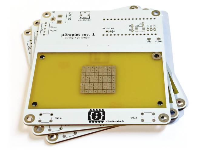 Unpopulated PCBs of µDroplet
I 3D-printed a base so that it stays level on a table, and a carrier frame for the hydrophobic/isolating material. The STL files are included in the repository.
Electrode array
The electrodes are responsible for the actuation of the droplets. Hence, their shapes are critical. For my platform, I copied the common "interlocking tiles" design. They are about 2.75×2.75 mm (volume of droplets: about 20 µL) [7].
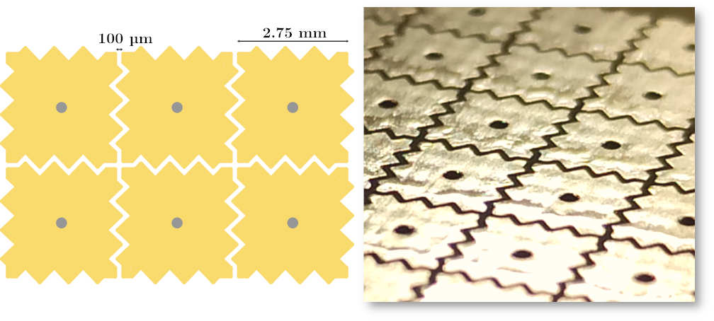 Left: render of the electrode array. Right: macro photograph of the electrode array on a PCB.
The overlap between pads makes it more reliable. Hence, the spacing needs to be as low as possible, the limit being the PCB manufacturing constraints. JLCPCB recommends a minimum pad-to-pad clearance of 0.127 mm (5 mils) in their manufacturing capabilities guidelines. However, the spacing in my electrode array is 0.1 mm (4 mils). They seem to have modified the gerber files to fit their constraints. 4 mils clearance often imply an additionnal cost (lower yields).
Solder mask is removed on top of the electrodes to expose them, allowing us to use a variety of diaelectric material. HASL surface finish is sufficient, but ENIG (immersion gold) is probably better for durability and better flatness. Similarly, plugged vias are not required, but would be an improvement.
Software
The microcontroller's firmware is very straightforward and drives the HV507 to enable or disable electrodes requested by the computer.
On the computer-side, we can control it with a serial port over USB, either manually or programmatically. I made a basic GUI in Processing to view the current status of the electrode array and to affect it:
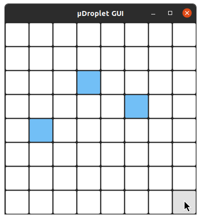 µDroplet control software, running on Processing 3 (blue cells = active electrodes)
Using this software, we can activate or deactivate the pads to move the droplets by clicking on the tiles or with the arrow keys. Pressing A activates the whole array and DEL does the opposite.
Usage and tests
The following section describes the preparation required to get started with µDroplet, and shows some test results.
Preparation
There are two main configurations for electrowetting-based systems: with a conductive top plate (usually, coated glass) or in "topless" configuration. The cover makes it more practical for lab use, and allows feedback/sensing. However, the topless configuration involves an easier setup. Hence, I will describe it here.
The objective is to lay a thin film of diaelectric material and coat it with an hydrophobic surface. This diagram shows the layers:
 Layer stackup for the open-top EWOD configuration
There is a variety of possible material for the diaelectric and/or the hydrophobic, with different properties: PTFE (teflon), ETFE, Polyimide, SiO₂, PDMS, etc [6].
The simplest setup to get started is:
- Diaelectric film: standard Parafilm® M from Bemis Company Inc.
- Hydrophobic coating: ELBESIL SILIKONÖL B 5 from Silikon Profis. This 5 cSt PDMS (silicone oil) has a very low viscosity, which makes it perfect for this application.
My procedure to prepare the array is [4]:
- Apply a thin film of silicone oil on the electrodes to prevent air from getting trapped between the diaelectric and the electrodes (about 15 µL for the array).
- Stretch a piece of Parafilm® in both directions. It needs to be as thin as possible without wrinkles or holes. Using a moderate amount of warm air makes the film less elastic, which makes this step easier.
- Apply the Parafilm® on top of the electrodes using the 3D-printed frame to keep it stretched.
- Apply another thin film of silicone oil on top of the Parafilm® to make it hydrophobic (about 15 µL for the array).
 µDroplet carrier frame with a stretched layer of Parafilm®, ready to use
Droplets can now be added on top of the electrodes. They should move easily on the surface. To remove any static charge, they should be poked with a grounded wire before the high voltage is applied (warning: this should never be done while the HV is on, it may destroy the driver if arcing occurs).
Moving a droplet
To move a droplet, the technique is straightforward: when we apply a voltage to an adjacent electrode, it will start stretching toward it, and the surface tension will pull it entirely [3].
This animation illustrates this effect:
Animation showing the movement of a droplet with the EWOD effect
The timing is not critical. The velocity of the droplet depends on:
- The diaelectric constant and the thickness of the film
- The voltage applied to the electrode
- The hydrophobicity of the diaelectric layer, and
- In the open configuration, the residual static charge of the drop
The relationship between these parameters is described by the fundamental equation for electrowetting:

Where θ is the contact angle under the externally applied electric potential V, θe is the equilibrium contact angle at V = 0 V, ε0 is the permittivity of vacuum, εd is the permittivity of the dielectric layer, γ is the interfacial tension between the droplet and the surrounding insulating fluid, and d is the thickness of the dielectric layer [4].
Moving a droplet
Following this procedure, I prepared the µDroplet device and programmed a single droplet to follow a repeating rectangular pattern:
Video clip demonstrating the movement of a single droplet on µDroplet
The threshold voltage to achieve reliable movement depend on the variables in the equation above. With the setup described here, it is about 150 to 200 V depending on how well the Parafilm® is stretched and how thick the oil layer is.
Since the control electrodes are insulated from the liquid, both ohmic heating and undesired electrochemical reactions should be prevented [3]. Hence, the alteration of the content of the droplet is minimal. However, such high voltage may degrade the insulator over time. An order of magnitude less (15-20V) is reachable with proper material and better driving techniques (including AC actuation) [1].
Moving multiple droplets
Of course, using the same technique, we can also control multiple drops of fluid simultaneously, as shown in this clip:
Video clip demonstrating the movement of multiple droplets on µDroplet
Conclusion
µDroplet can be built for under $40. It is a simple learning platform to experiment with electrowetting, allowing to adjust various parameters. I achieved fast and reliable control of the droplets in the open configuration, albeit using high voltage.
Of course, there is a lot of room for improvement from this first version. For instance, the shape of the electrodes array could be modified to include some of the more complex structures, like reservoirs/sinks. I plan to work on an improved version in the future.
To go further, the team at GaudiLabs has been working for years on their open-source "OpenDrop" [9]. It is a more complex but much more capable platform with true AC driving capability, optical isolation, a modular cartridge system and embedded UI.
Downloads
µDroplet is published on GitHub: https://github.com/CGrassin/microdroplet_electrowetting
This repository archives all files required to build µDroplet, including the source files.
Bibliography/references
- Nagiel, I. (2007). AC Electrowetting Actuation of Droplets on a Digital Microfluidic Platform. Department of Electrical and Computer Engineering, Pratt School of Engineering, Duke University. http://citeseerx.ist.psu.edu/viewdoc/download?doi=10.1.1.539.1011&rep=rep1&type=pdf. ↩
- Fair, R. B. (2007). Digital microfluidics: is a true lab-on-a-chip possible?. Microfluidics and Nanofluidics, 3(3), 245-281. https://doi.org/10.1007/s10404-007-0161-8. ↩
- Pollack, M. G., Shenderov, A. D., & Fair, R. B. (2002). Electrowetting-based actuation of droplets for integrated microfluidics. Lab on a Chip, 2(2), 96-101. https://doi.org/10.1039/B110474H. ↩
- Chae, J. B., Lee, S. J., Yang, J., & Chung, S. K. (2015). 3D electrowetting-on-dielectric actuation. Sensors and Actuators A: Physical, 234, 331-338. https://doi.org/10.1016/j.sna.2015.09.004. ↩
- Welch, E. R. F., Lin, Y. Y., Madison, A., & Fair, R. B. (2011). Picoliter DNA sequencing chemistry on an electrowetting‐based digital microfluidic platform. Biotechnology journal, 6(2), 165-176. https://doi.org/10.1002/biot.201000324. ↩
- Liu, H., Dharmatilleke, S., Maurya, D. K., & Tay, A. A. (2010). Dielectric materials for electrowetting-on-dielectric actuation. Microsystem technologies, 16(3), 449. https://doi.org/10.1007/s00542-009-0933-z. ↩
- Urs Gaudenz (2016, April 26). New Electrode Design, from https://www.gaudi.ch/OpenDrop/?p=76. ↩
- GaudiLabs (2020, June 25). Do It Your Self Electrowetting Coating for OpenDrop Cartridge, from https://www.youtube.com/watch?v=xyblkFywYIk.
- Alistar, M., & Gaudenz, U. (2017). OpenDrop: An integrated do-it-yourself platform for personal use of biochips. Bioengineering, 4(2), 45. https://doi.org/10.3390/bioengineering4020045. ↩
Auteur : Charles Grassin
What is on your mind?
Sorry, comments are temporarily disabled.
#1 phil
on September 22 2024, 16:31