Foreword on VHDL
After a FPGA/VHDL course I followed during my engineering education, I decided to try to design my custom microprocessor architecture. This learning experiment is described in this article. All of the code is available on my GitHub (link at the bottom of the article).
VHDL (VHSIC Hardware Description Language) is an IEEE standard hardware description language. It describes architectures and behaviors, which means that it determines how some logic gates will be connected. This is very different for a programming language, say C++, where the compiled code is sequentially executed by a CPU.
For instance, the VHDL statement a <= b and c; will, in the case of FPGAs, physically implement an AND logic gate, taking as input the b and c signals, and having as output another signal a. This is fundamentally different from the C instruction a = b & c; that asks the processor to do the b AND c instruction, and then put it in the a variable/register.
VHDL, which is not the only hardware description language, belongs to electronics realm more than software programming.
Note: all the VHDL code for this project is pure "dataflow", without using so-called "processes". This makes it very much a direct translation of the figures hereunder. Hence, it is very close to the hardware/electronics implementation.
The architecture definition
Before describing the processor in VHDL, we need to define the architecture that will be implemented. This step was an iterative process, during which, by drawing the functionnal blocks and their implementation, we can figure out the errors and limitations of the design.
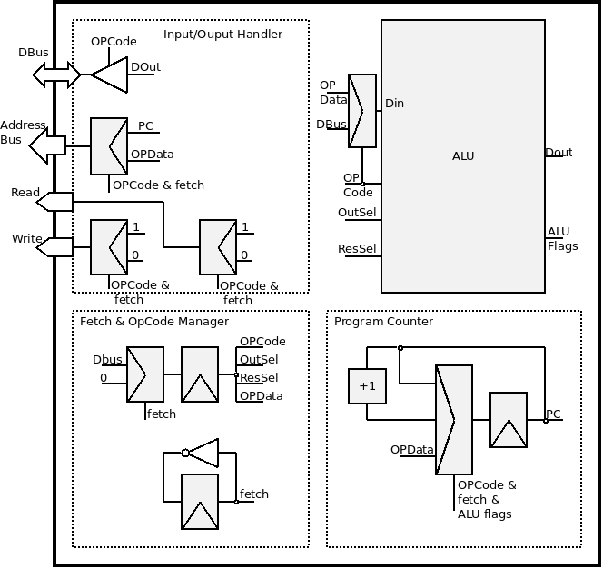
My final model is the following:
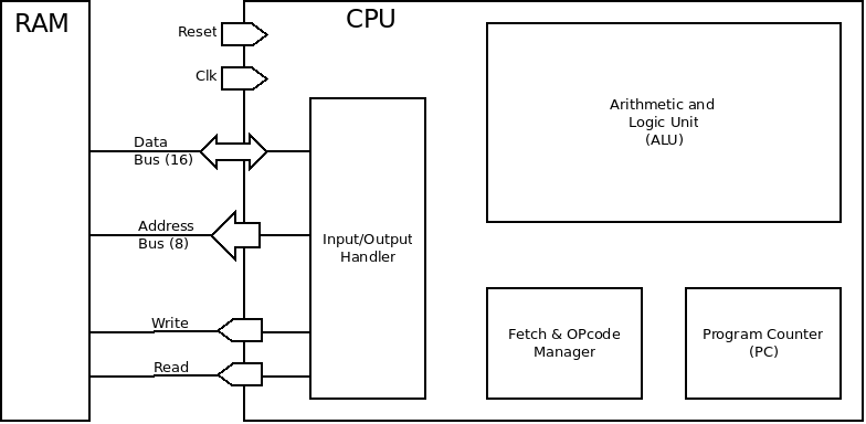
Let's define the main elements:
- The Fetch & OpCode Manager loads the instructions in memory and passes them to the ALU and the rest of the system,
- The Progam Counter (PC) holds the address of the next instruction to load by the Fetch & OpCode Manager. It increments at each cycle, but may be altered by some instructions (such as a GoTos),
- The Arithmetic and Logical Unit (ALU) is the processor's heart: it does arithmetical (plus, minus, etc.) and logic (AND, OR, etc.) operations on its registers,
- The Input/Output Handler is controlled by the Fetch & OpCode Manager. It chooses the states of the inputs and outputs. For instance, it may connect the output of the ALU to the data bus, put the content of the PC in the address bus, etc.
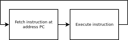
Two cycles execute alternately:
- The processor gets an instruction from memory at the address PC. This is fetch,
- It executes this instruction. It may be a arithmetic/logic operation, a data operation with RAM or a flow control operation.
When designing the architecture, we need to define an instruction set and how they are structured in memory. This instruction set is everything the CPU can do. I chose my instructions to be layed out like this, in binary representation:
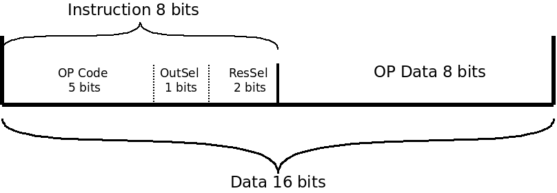
The length is fixed to 16 bits, and the execution time to one CPU cycle (or two, if we include the fetch). The OP Data field contains the parameters of the operation. The OutSel and ResSel fields will be described in the ALU chapter. For now, if we focus on the OP codes:
| Nom | OPCode | Description |
|---|---|---|
| NOP | 00000 | Does nothing (No OPeration) |
| Get.X @ | 00001 | Fetchs the content of the X register to the @ address of the memory |
| Set.X @ | 00010 | Puts the content of the address @ in the X register (opposite of Get) |
| SetL.X Y | 00011 | Puts the value Y (on 8 bits) in the X register. The value is a constant/literal, unlike "Set" |
| Goto @ | 00110 | Unconditional jump: put the address @ in the PC, meaning that the next instruction will be fetched at address @ instead of PC+1 |
| GotoIfNull.X @ | 0010X | Conditional jump: put the address @ in the PC if register X equals 0 |
| Inc.X | 0100X | Increments the register X |
| Dec.X | 0101X | Decrements the register X |
| Add | 00111 | Adds both registers together |
| Sub | 01100 | Subtracts both registers together |
| And | 01101 | Does a logic AND between registers |
| Or | 01110 | Does a logic OR between registers |
These instructions where chosen to have a sufficient number of functions to make a Turing complete computer.
The Arithmetic and Logic Unit (ALU)
The ALU is the functional block of the CPU that actually does the calculations. It acts on two registers in which we can put a value, do computations et get the result.
Architecture
This is my ALU's architecture:
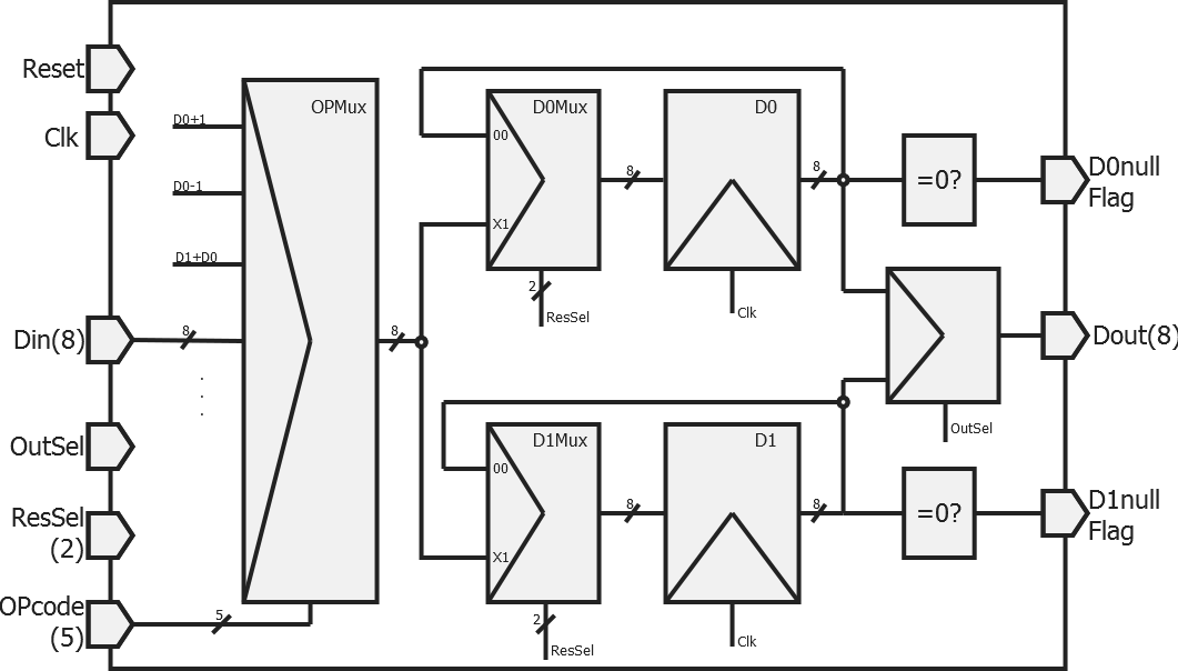 All registers are suposed to be connected to an asynchronous reset, and active on a rising clock edge.
It works like this:
- The OPMux is the multiplexer that chooses the operation. As input, we get all possible operations, while the output selects the appropriate result based on the OPcode.
- The registers D0 and D1 contain the variables used by the processor, that are the operands of the ALU.
- The multiplexers D0Mux and D1Mux choose if the result of the operation is copied to the register, or if it is unaffected.
- The flags are Boolean output (true/false) that allow us to check a conditional statement: D0/D1=0? This enable us to do conditional jumps like "Go to address @ if D0=0".
- Finally, the last multiplexer chooses the register connected to an output.
To add new operations, we would simply need to add a new input to the multiplexer OPMux. The OPCode is, by my own definition, on 5 bits, we have a total of 2^5=32 possible codes.
Note: The output of the ALU is only used by the "Get" command. The OutSel bit is only used in that case. We could easily use that bit for extra operations. Therefore, we have, in theory, 2^6-1=63 possible codes. However, for the sake of simplicity and using a minimal number of gates, I kept this kind of optimizations aside.
VHDL Code
I obviously won't detail my entire VHDL code. However, I wanted to go over some interesting blocs.
Asynchronous multiplexers can be written like this:
mux <= input0 when Sel=sel0 else input1 when Sel=sel1 else .... ;This means to connect the output wire "mux" to one input, depending on the selector "Sel". For instance, for OPMux, its inputs are mathematical operations, and the selector is the OPCode.
A register with its multiplexer is written like this:
D0Mux <= OPMux when Sel='1' else D0; --mux
D0 <= ( others => '0' ) when reset='1' else D0Mux when rising_edge(clk); --register
The register copies the input (D0Mux) at every rising edge of the clock, and keeps it until the next rising edge. The input multiplexer selects whether we want to feed the output back on itself (keep the value), or alter it with a signal (D0, here).
We only synchronize register on clock edges. The combinatory signal therefore have exactly one clock period to get stable. The implication is that there is a frequency cap, that depends on the maximum stabilization/propagation time in the combinatory part between two synchronous registers. This characteristic will be later studied at the CPU scale, in the conclusion of this project.
Tests and validation
The other critical part, after the architecture definition, is the unitary test of functional blocs. The Xilinx ISE Webpack suite that I used for this project includes a simulator, ISim, that allow us to virtually connect the input of logic gates to arbitrary signals, and probe the output. Simulation is a fundamental part of VHDL: some commands only work on this mode.
To test the ALU, I injected signals into its inputs to analyze the result. For instance:
OpCode <= OPCodeINC0;  --Increment D0
ResSel <= "01";        --Put result to D0
OutSel <= '0';         --Set output to D0
The output is the following, when also defining a clock and an initial reset:
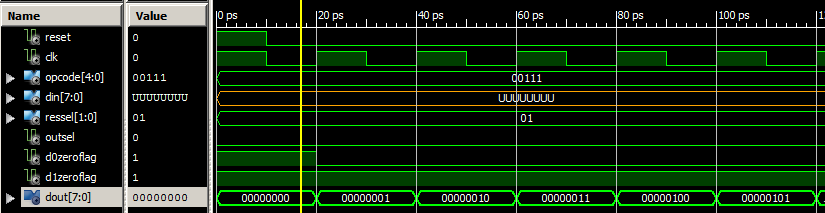
We clearly see, on the output DOut, the incrementation on each clock (clk) rising edge. I ran other simulations to validate my design, before adding the control circuitry, to obtain a working CPU.
The CPU
Architecture
Defining the CPU's architecture is deciding of the implementation of each of the control blocs we previously defined. The complete diagram, that stays surprisingly simple, is the following:
 Reset and clock input are not shown. The "&" input of the multiplexers indicate that the output is selected by a combination of all of the mentioned signals.
Again, we will describe the blocs one by one to explain the flow:
- The Fetch & OpCode Manager handle the alternation between the fetch cycle and the execution of the instruction. It stores the instruction after each fetch. It also decomposes the instruction in its atomic bits, used by the rest of the CPU (including the ALU). Note that it takes the value zero during the fetch, which correspond to the NOP, so that the rest of the system does not carry on the previous instruction.
- The Program Counter has a single output: the address of the next instruction to fetch. It changes at each clock rising edge, to 3 possible values:
- PC + 1, always after a fetch,
- PC (no change), always after an instruction cycle, except in the following case,
- OP Data, when a jump (conditional or not) is performed. It may depend on some ALU flags.
- The ALU was detailed in the previous chapter.
- The Input/Output Handler chooses the states of the ports. For instance, if the OPCode is a Get, it puts Read to 0, Write to 1, the address to OPData and connects the data bus to the ALU's Dout.
VHDL Code
This code uses the same building blocs that were previously defined. However, I will showcase the code of the buffers that decides the state of DBus.
If we were using the following code:
dataBus <= Dout when OPCode=OPCodeGET else (others => '0');If the OPCode was a Get, we would connect the bus the the output Dout of the ALU, but in any other situation (a fetch, for instance), if a peripheral was trying to use the bus, a single '1' (VCC) would directly connect to the '0' (GND) that we are forcing: this is a short-circuit!
To avoid this situation, we use the third state, 'Z', that stands for high impedance. This means that we don't connect the signal to anything. The other bus other can put a '0' or a '1' without any issue. The code for this tri-state buffer is therefore:
dataBus <= Dout when OPCode=OPCodeGET else (others => 'Z');Tests and validation
Testing the whole CPU is a lot trickier than the unitary tests of the ALU. There are indeed a lot more internal states, and there is more room for design or coding errors. To solve this issue, as a first step, I ran some unitary tests by injecting each instruction in the CPU, before testing more complex algorithms with conditional jumps and nested calculations.
For instance, the following screenshot corresponds to a simple SetL on the D0 and D1 registers:
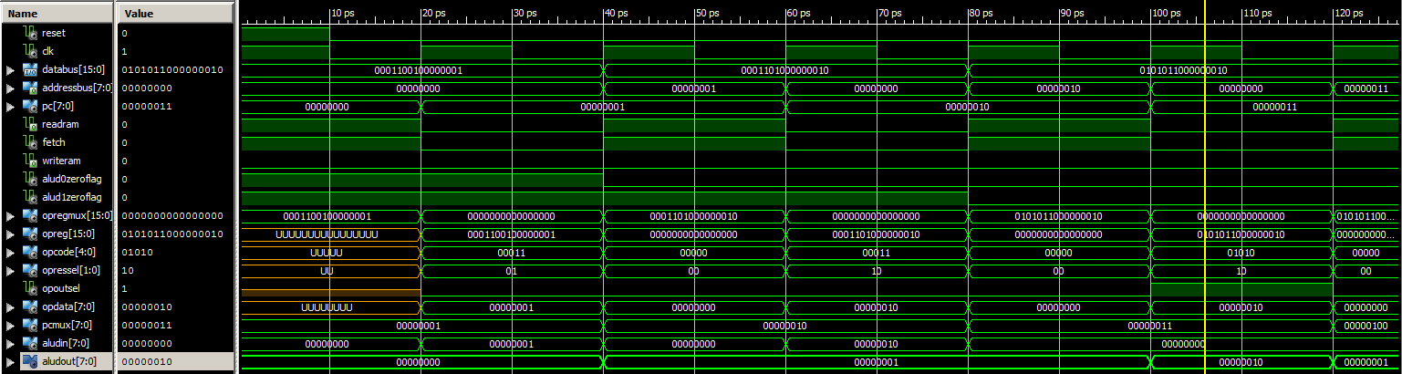
Obviously, we won't go into details on the waveform, but we easily notice the alternation between the fetch and instruction cycles, with the fetch signal. We also notice the incrementation of PC after each fetch.
A careful analysis of these simulations validates the CPU design and code.
From microprocessor to computer
Adding RAM
To actually "use" this CPU out of the ISim simulation, we need to add memory to store variables and instructions. To do this, I made the following VHDL module that controls a memory (a list of registers). It matches with the processor's architecture: 16 bits words, 8 bits addressing, a read and a write. This figure describes the module:
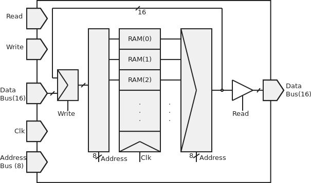
The "DataBus" port is drawn twice because it is bidirectional: used both as input and output.
The idea is simple (the VHDL code is only 3 lines!):
- If Read=1, we put the content of the register, called by address, to the data bus. If Read=0, the output is set to the 'Z' state.
- If Write=1, we put the content of the data bus in the register, called by address. If Write=0, this register is set to its own value.
For security, in the VHDL description, these two notions are mutually exclusive: Read=Write=1 is strictly equivalent to Read=Write=0
This is the simplified VHDL code, for this (RAMbuffer is the left multiplexer on the diagram):
dataBus <= RAM(addressBus) when  ReadRAM='1' else ( others => 'Z' );
RAMbuffer <= dataBus when WriteRAM='1' else RAM(addressBus);
RAM(addressBus) <= RAMbuffer when rising_edge(clk);
Programming the machine
To actually use this "computer", we simply need to put a program and its data into RAM. Of course, this needs to be in machine language (binary).
For instance, the program hereunder:
- Initializes a number to 10,
- Increments it as long as it is different than 20,
- Decrements it as long as it is different than 0, and starts over.
0001100100001010 0001101000010100 0110001000000000 0010100000000110
0100000100000000 0011000000000001 0010000000000001 0101000100000000
0011000000000110
This is utterly unreadable. To solve this issue, I also coded an assembler for my instruction set. It's an AWK script that takes as input an assembly language file (according to the specification above), and that creates the binary machine language. It support some basic assembly functions: labels, comments, etc.
For instance, the program above can be written:
SetL.0 10       ;Init Reg0 to 10

increment:
SetL.1 20       ;Put 0 in Reg1
Sub.1           ;Reg1=Reg1-Reg0
GotoIfNull.1 decrement ;if Reg1=0...
Inc.0           ;else, increment Reg0
Goto increment  ;restart (until Reg0=20)

decrement:
GotoIfNull.0 increment ;if Reg0=0...
Dec.0           ;else, decrement Reg0
Goto decrement  ;restart (until Reg0=0)
Much easier! We can now, finally, implement the processor on silicon!
Physical implementation on an FPGA
To give a practical dimension to theis project, I decided to implement it on a FPGA (field-programmable gate array). This is a network of logic gates that can be "connected" together, based on the VHDL description. The process of going from a VHDL code to a matrix of interconnected gates is known as silicon compilation.
I used a Digilant Basys2 education development board, which includes a Xilinx Spartan-3E (100 000 logic gate)
If I only configured the FPGA with my PU in its RAM, it would run, but we would not be able to see anything because there would be no visible output. To see the CPU working, I created a very simple program that increments a register of the RAM, and I connected this register to physical pins of the FPGA (LEDs). The clock is wired to a very slow 60 Hz, and the asynchronous reset to a physical switch.
This video shows this configuration running:
This is the assembly code for the program used in the video (LEDs are on the bottom of the board, just above the switches):
SetL.0 0    ;init reg0 to 0
loop:
Inc.0       ;increment reg0
Get.0 4     ;RAM(4)=reg0
Goto loop   ;infinite loop
0           ;RAM(4), hard wired to the LEDs
Conclusion
CPU Performance
Not that it really matters, but it is interesting to look at the performance of the processor nonetheless:
- All instructions execute on a constant period of two clock cycles, and are on 16 bits.
- The worst case propagation time on the Spartan-3E chip is 7ns. This corresponds to a maximum clock frequency of 150MHz, or 75,000,000 instructions per second. However, this frequency is highly dependent on the FPGA and silicon compiler.
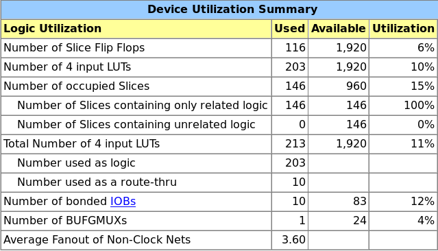
- We need very few logic gates to implement the processor. The following capture shows the device utilization of the chip:
- As it is built, most of the 256 possible instruction codes are consumed by the OutSel and ResSel fields. From the 8 bits, we only get 32 usable code in the end. This choice was made on purpose to avoid having to add more complexity and gates. To circumvent it, we would simply have to add a few selectors and multiplexers.
- Worst, 50% of the memory is not usable because the ALU is on 8 bits while the bus is 16 bits wide...
To go further
During the design of this processor and the redaction of this article, there is a number of ideas I had to improve this architecture:
- Fix the problem of the 50% of unusable memory. The better approach is to have an 8 bits wide memory, and to fetch N consecutive times to get the full instruction and data. The simpler approach is to have two separate RAM/ROM: one 16 bits wide for the instructions, and one 8 bits wide for the data.
- Outside of simplicity, the form of the instructions with the ResSel and OutSel fields does not make much sense. It gives the possibility to do weird things, such as incrementing a variable without saving the result or zero a variable while doing a GoTo. This can be fixed by adding a bit of logic to the Fetch & OpCode Manager so that it handles those internal fields.
- Add features! Interrupts, hardware stack, more instructions, GPIOs, etc.
- Going toward a pipelined architecture: fetching the next instruction while the current one it being executed.
Download
Go to my GitHub repository to download the source for this project (VHDL and assembler): https://github.com/CGrassin/vhdl_cpu
Author: Charles Grassin
What is on your mind?
Sorry, comments are temporarily disabled.
No comment yet!